Analyzing Temperature Parameters of Si, SiC and GaN Power Devices
| Topics covered in this article: |
| Ⅰ. Si family of Power devices |
| Ⅱ. SiC family of Power devices |
| Ⅲ. Depletion Mode GaN Power Devices and Enhancement Mode GaN Power Devices |
| Ⅳ. Conclusion |
Although wideband gap (WBG) power devices, such as SiC MOSFETs and GaN HFETs, offer remarkable material advantages over traditional Si devices, their growing application and interest arise from their superior properties and commercial viability. Enhanced by a 10X higher electric field strength, SiC devices exhibit significantly improved Figure of Merits (FOMs), enabling size reduction by up to 65 times compared to Si MOSFETs.
The size reduction leads to reduced parasitic capacitance and higher switching speeds, promising megahertz-range operation for power MOSFET converters. However, this downsizing also brings about thermal management challenges, as increased device thermal impedance necessitates precise sensing of junction temperature to avert thermal runaway.
Different methods of temperature sensing, such as NTC resistors and online junction temperature-sensitive electrical parameters (TSEP) techniques, are under examination to optimize efficiency in such devices. Despite previous research, it is essential to comprehensively assess and compare devices from different manufacturers accurately with an aim to develop improved strategies for online temperature monitoring enhancing the reliability of high-power modules.
Ⅰ. Si family of Power devices
Si Power MOSFET and the SuperJuction Power MOSFET (CoolMOS): High-voltage Si power MOSFETs use a D-MOSFET structure. Key resistances include source contact (RCS), source region (RN+), channel (RCH), accumulation (RA), JFET (RJFET), drift region (RD), N+ substrate (RSUB), and drain contact (RCD). For 1000V Si MOSFETs, RD and RCH dominate, varying with temperature. Their temperature dependency relies on resistivity (ρ) and electron mobility (μ). Channel length (LCH) and cell length (Z) matter. The threshold voltage (Vth) depends on P-region doping (NA), oxide capacitance (Cox), and charge (Qox). Intrinsic carrier concentration (ni) impacts Vth inversely due to its ln-based role. Gate-to-source equivalent impedance includes internal resistance (Rg,int), and gate capacitance involves CGN+ and CGP, tied to N+ and P regions respectively, as shown in Figure 1.
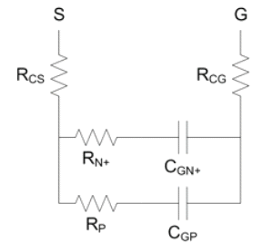
Fig 1 Equivalent impedance circuit of gate to source in Si MOSFET.
On the other hand, the CoolMOS is a device that enhances the planar DMOS structure by introducing a vertical P-N junction. Its higher doping concentration in the drift region compared to conventional power DMOS design, provides a reduced on-state resistance (Rds,on). The resistance components include the source contact, source region, channel, accumulation, drift regions 1 and 2, N+ substrate, and drain contact, while Vth and Rg,int remain akin to Si MOSFET.
Si IGBT: Modern high-voltage Si IGBTs employ a field stop trench-gate structure. The on-state voltage drop comprises VP+N (P+ collector/N-base junction), VNB (N-base region voltage drop considering high-level injection effects), and VMOSFET (MOSFET part voltage drop). Si IGBT shares Si D-MOSFET's Vth and Rg,int, differing in trench gating.
Ⅱ. SiC family of Power devices
• SiC MOSFET: Currently, SiC power devices are primarily made in planar-gate configuration, with a few in trench-gate design. While their Ron and Vth equations resemble Si MOSFETs, they differ in material-related parameters. Notably, SiC MOSFET's channel mobility rises with temperature, unlike Si MOSFET which decreases. Both devices see reduced drain mobility with higher temperatures. Unlike Si, SiC experiences minimal dopant diffusion due to implantation.
• SiC JFET: SiC JFETs now mostly adopt trench-gate designs, differing from SiC MOSFETs. Their Ron lacks accumulation resistance (RA) as in SiC MOSFETs due to their normally-on nature. The channel remains conductive without gate bias. The gate-to-source equivalent impedance includes channel resistance (RCH). Capacitances CP+N- and CN+P+ exist between P+ and N- regions and between P+ and N+ regions, respectively, as illustrated in Figure 2.
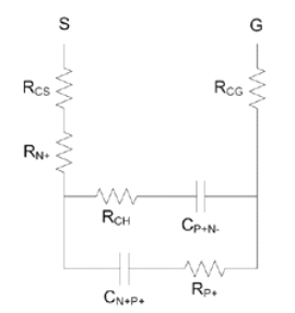
Fig 2 Equivalent impedance circuit of gate to source in SiC MOSFETs.
Ⅲ. Depletion Mode GaN Power Devices and Enhancement Mode GaN Power Devices
Depletion-mode GaN power devices are commonly cascoded with low-voltage Si MOSFETs. Their characteristics, such as Rg,int and Vth, resemble Si MOSFETs. The Ron of GaN HEMTs is described by LD (gate-drain spacing) and ns (2D electron density).
On the other hand, enhancement-mode GaN power devices uses a gate depletion region. This design makes sure that the device remains in an off-state without gate potential, removing the drain-source connection through the 2D electron gas.
Characterization Methods and Results
• Rg,int Characterization: Figure 3 illustrates the overall impedance of vendor C's SiC MOSFET across a 5~100MHz range. It was seen, at 27.5MHz, the impedance curve reflects the series resistance (Rg). Vendor A's Si MOSFET and Si IGBT exhibit temperature-dependent Rg behavior: increasing until approximately 75°C and then decreasing. Meanwhile, vendor D's SiC JFET displays significantly inferior Rg characteristics compared to vendor A's Si MOSFET and Si IGBT. This hinders its viability as a thermal sensing element (TSEP).
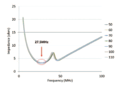
Fig 3 Tj-Impedance relation of SiC MOSFET.
• Onstate Resistance (Ron) Characterization: Figure 4 illustrates that the 1200V Si MOSFET has the highest Ron at 80 ohms, while the other 6 devices exhibit Ron below 1 ohm. Among these, the 650V CoolMOS has the greatest Ron, whereas the 650V eGaN HEMT boasts the smallest. CoolMOS exhibits the highest Tj coefficient at 0.6 ohms/°C, while GaN HEMT cascode shows the lowest at 0.2 ohms/°C. Also, the Tj coefficient range for Ron across all devices was seen to be around 0.4~0.6 ohms/°C.
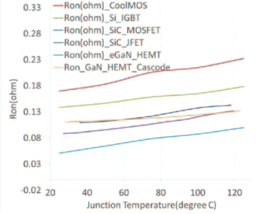
Fig 4 6 devices under different Tj and their Ron.
• Threshold Voltage (Vth) Characterization: The threshold voltage (Vth) assessment was conducted on various devices except for the SiC JFET, which remains normally on. In this evaluation, the gate and drain were shorted. Figure 5 illustrates a close-up of the Ids-Vgs curve for Vth measurement of the GaN HEMT Cascode. Among Wide Bandgap (WBG) devices, the SiC MOSFET exhibited the lowest Vth, approximately 11.2V. The tested eGaN HEMT followed closely, displaying a temperature-dependent fluctuation, unsuitable for TSEP. Another 100V eGaN HEMT from the same manufacturer with a linear Tj coefficient yielded a Vth of 2.22.4V for the GaN HEMT Cascode, primarily dictated by the low voltage Si MOSFET.
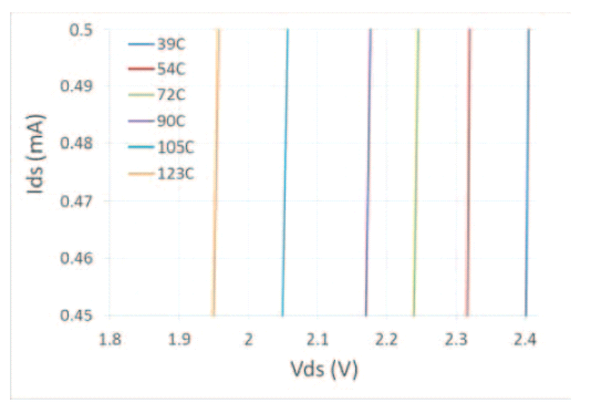
Fig 5 Characterized Ids-Vds curve for measuring Vth.
Ⅳ. Conclusion
An experiment was done to study three TSEPs – internal gate resistance (Rg,int), on-state resistance (Ron), and threshold voltage (Vth) – in different Si, SiC, and GaN power devices.
Ron and Vth exhibited more favourable temperature coefficients for Wide Band Gap (WBG) devices compared to Si. However, using them as TSEPs for WBG applications requires enhanced sensing technology and higher sampling rates due to faster switching. Temperature coefficients of Rg,int varied significantly among manufacturers and proved relevant for only a few devices, warranting careful consideration in its application.
 Discovering New and Advanced Methodology for Determining the Dynamic Characterization of Wide Bandgap DevicesSaumitra Jagdale15 March 20242495
For a long era, silicon has stood out as the primary material for fabricating electronic devices due to its affordability, moderate efficiency, and performance capabilities. Despite its widespread use, silicon faces several limitations that render it unsuitable for applications involving high power and elevated temperatures. As technological advancements continue and the industry demands enhanced efficiency from devices, these limitations become increasingly vivid. In the quest for electronic devices that are more potent, efficient, and compact, wide bandgap materials are emerging as a dominant player. Their superiority over silicon in crucial aspects such as efficiency, higher junction temperatures, power density, thinner drift regions, and faster switching speeds positions them as the preferred materials for the future of power electronics.
Read More A Comprehensive Guide to FPGA Development BoardsUTMEL11 September 202515474
This comprehensive guide will take you on a journey through the fascinating world of FPGA development boards. We’ll explore what they are, how they differ from microcontrollers, and most importantly, how to choose the perfect board for your needs. Whether you’re a seasoned engineer or a curious hobbyist, prepare to unlock new possibilities in hardware design and accelerate your projects. We’ll cover everything from budget-friendly options to specialized boards for image processing, delve into popular learning paths, and even provide insights into essential software like Vivado. By the end of this article, you’ll have a clear roadmap to navigate the FPGA landscape and make informed decisions for your next groundbreaking endeavor.
Read More Applications of FPGAs in Artificial Intelligence: A Comprehensive GuideUTMEL29 August 20253773
This comprehensive guide explores FPGAs as powerful AI accelerators that offer distinct advantages over traditional GPUs and CPUs. FPGAs provide reconfigurable hardware that can be customized for specific AI workloads, delivering superior energy efficiency, ultra-low latency, and deterministic performance—particularly valuable for edge AI applications. While GPUs excel at parallel processing for training, FPGAs shine in inference tasks through their adaptability and power optimization. The document covers practical implementation challenges, including development complexity and resource constraints, while highlighting solutions like High-Level Synthesis tools and vendor-specific AI development suites from Intel and AMD/Xilinx. Real-world applications span telecommunications, healthcare, autonomous vehicles, and financial services, demonstrating FPGAs' versatility in mission-critical systems requiring real-time processing and minimal power consumption.
Read More 800G Optical Transceivers: The Guide for AI Data CentersUTMEL24 December 20254378
The complete guide to 800G Optical Transceiver standards (QSFP-DD vs. OSFP). Overcome supply shortages and scale your AI data center with Utmel Electronic.
Read More Xilinx FPGAs: From Getting Started to Advanced Application DevelopmentUTMEL09 September 20254396
This guide is your comprehensive roadmap to understanding and mastering the world of Xilinx FPGA technology. From selecting your first board to deploying advanced AI applications, we'll cover everything you need to know to unlock the potential of these remarkable devices. The global FPGA market is on a significant growth trajectory, expected to expand from USD 8.37 billion in 2025 to USD 17.53 billion by 2035. This surge is fueled by the relentless demand for high-performance, adaptable computing in everything from 5G networks and data centers to autonomous vehicles and the Internet of Things (IoT). This guide will walk you through the key concepts, tools, and products in the Xilinx ecosystem, ensuring you're well-equipped to be a part of this technological revolution.
Read More
Subscribe to Utmel !
![CS8190ENF16G]() CS8190ENF16G
CS8190ENF16GON Semiconductor
![AD9267BCPZRL7]() AD9267BCPZRL7
AD9267BCPZRL7Analog Devices Inc.
![EL3021]() EL3021
EL3021Everlight Electronics Co Ltd
![L9654]() L9654
L9654STMicroelectronics
![LTC3725EMSE#PBF]() LTC3725EMSE#PBF
LTC3725EMSE#PBFLinear Technology/Analog Devices
![FOD410V]() FOD410V
FOD410VON Semiconductor
![LTC4213CDDB#TRMPBF]() LTC4213CDDB#TRMPBF
LTC4213CDDB#TRMPBFLinear Technology/Analog Devices
![CAP005DG-TL]() CAP005DG-TL
CAP005DG-TLPower Integrations
![AD9970BCPZRL]() AD9970BCPZRL
AD9970BCPZRLAnalog Devices Inc.
![AT88SC0808CA-MJTG]() AT88SC0808CA-MJTG
AT88SC0808CA-MJTGMicrochip Technology


 Product
 Brand
Brand Articles
 Tools
Tools


